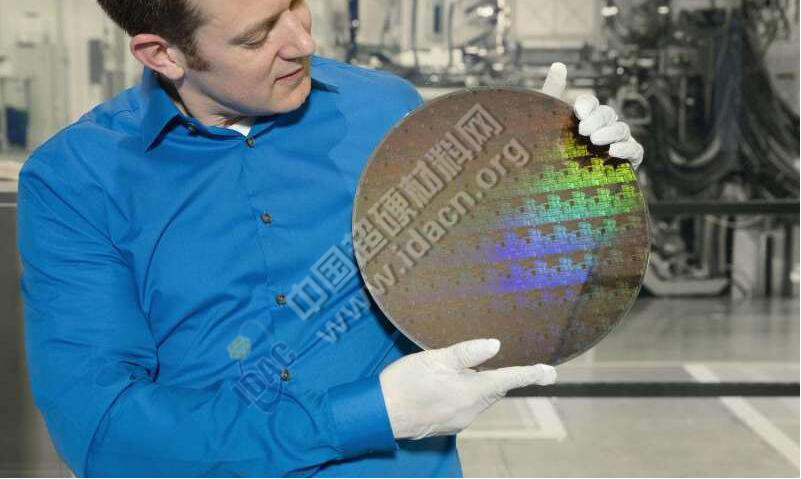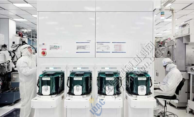
This technology will greatly improve the performance of intelligent computing, IoT and data-intensive devices; and the energy efficiency will greatly increase the battery life of smartphones and other mobile devices by two to three times.
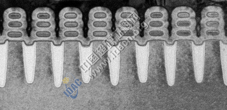
Scientists have replaced the FinFET structure (standard fin field effect transistor) with stacked silicon nanosheets as a transistor device structure. The FinFET structure was previously a blueprint for 7nm thin chip technology.
The future economic and social development has great demand for intelligent computing and cloud computing, and the innovation and promotion of semiconductor technology play an important role in it. Arvind Krishna, senior vice president and head of the IBM research group, said: Based on the requirements and promotion of this big environment, IBM is actively exploring new and unique structural technologies and new materials to promote innovation in the semiconductor industry.

Compared with the current 10nm mainstream technology on the market, the 5nm size thin film technology can enhance 40% performance under fixed power conditions, and can save 75% energy under matching performance conditions. This technology greatly caters to the future development requirements of artificial intelligence systems, virtual reality and mobile devices.

The nanoflake transistor structure in this study uses Far Ultraviolet Lithography (EUV), which enables continuous adjustment of nanosheet widths, either within a single manufacturing process or within the wafer design flow. This tunability technique can fine-tune the performance and power of a particular circuit, which is not currently available in FinFET transistor fabrication processes, and it is the current-loading scale of FinFET transistors that limits the breakthrough and development of the process. Therefore, even if the FinFET wafer can achieve a size of 5 nm, simply shrinking the space between the scales does not effectively increase the current and provides an additional performance improvement. ( Compile: China Superhard Materials Network )
company is one of the key enterprises of state machinery industry,specialized and sales in shearing,press brake,Rolling Machine,Hydraulic Press,levelling machine,metallrgical equipment.The centers,etc.More than 100setsof high-precision processing equipment,greatly improving quaity of products and meeting the custmers demands.Meanwhile,there are various sales service department in each province in whole country,for promot and convenient service to the custmer.
First-class design technology requires advanced processing technology to ensure the manufacture of high-quality sheet metal equipment. Our company has introduced a number of precision machine tools imported from abroad, including large floor boring and milling machines, gantry type, vertical and horizontal machining centers, CNC lathes, CNC laser cutting machines, precision large plane, cylindrical and guideway grinders, etc. At the same time, it has key testing equipment such as vibration aging, high-frequency heat treatment and API laser interferometer to ensure product processing accuracy and assembly quality.
Shearing Bending Machine,Shearing Machine,Bending Machine,Cnc Bending Machine
Rugao Yaou Import & Export Trade Co., Ltd , https://www.ntyaous.com