1 Introduction
Diamond is currently the hardest material for industrial production, and it is widely used as a processing and grinding material by its hardness characteristics. However, in addition to its high hardness, many of its excellent properties have been discovered and excavated, such as high thermal conductivity at room temperature, very low coefficient of thermal expansion, low coefficient of friction, good chemical stability, and large forbidden band width (5.5). eV), high acoustic propagation velocity, doping-induced semiconductor properties, and high optical transmittance make it a promising application in many fields such as machining, microelectronic devices, optical windows, and surface coatings. Therefore, the research and application of the functional properties of diamond materials have aroused great interest and made breakthroughs and progress in many fields.
2. Research and application in wide bandgap semiconductors
As a wide-bandgap semiconductor, diamond is undoubtedly the most attractive application prospect in optoelectronics. However, due to the difficulty in doping n-type diamond semiconductors, the difficulty in preparing homojunctions has increased. Currently, the leading research is on the pn junction of diamond thin films at MIT. Koizumi of MIT in 2001. The diamond film pn junction was prepared for the first time, and two diamond films were prepared by homoepitaxial growth on the (111) plane of the diamond single crystal. The p-type semiconductor was formed by doping diamond film with B element, n-type. The semiconductor was prepared by doping with P element, and then they improved the device. Under the application of a 20V bias circuit, the device was excited to emit ultraviolet light, and it was pointed out that the device can operate at high temperatures.
Alexov A et al. prepared a layer of N-doped diamond film on the diamond film doped with B element by homoepitaxial method, but the characteristics of electroluminescence of the pn junction were not reported in detail. Subsequent reports on homojunctions are very uncommon, and it is estimated that there are some difficulties due to the repeatability of diamond n-type semiconductor doping. Currently, reports are focused on diamond semiconductor heterojunctions, for example, A B-containing diamond film is grown on the Si wafer, or Schottky diodes and Field effect transistors (FETs) are prepared.
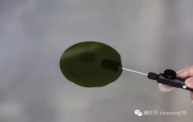
The method of preparing B-containing diamond film by chemical vapor deposition (CVD) method in 1987 is not perfect, so Geis et al. prepared the first diamond Schottky diode contacted by W element by synthesizing B-containing diamond single crystal. The performance of the sample was examined at °C, and the sample was determined to have a high breakdown field strength. Relevant personnel of the same subject group further investigated the effects of different metal element contacts on the performance of diamond Schottky diodes. A large number of work showed that Al, Au, and Hg elements were used as surface contact elements of B-containing diamonds, and Schottky diodes were used. Performance has a more positive effect, annealing or forming conductive carbides on the diamond surface can form a good ohmic contact on the surface of the diode.
Chen and Butler have done a lot of work on the performance improvement of Schottky diodes, and the samples prepared by Butler have a breakdown field strength of more than 6kV and have attracted much attention. After the CVD method for the preparation of diamond thin films matured, especially after the successful preparation of nano-diamond films, the research on diamond Schottky diodes began to be refined and continued to this day.
A field effect transistor (FET) is also a type of transistor that participates in conduction, also called a unipolar transistor, and is a voltage-controlled semiconductor device. Diamond's high carrier mobility, high breakdown field, high thermal conductivity, high power characteristics can be inferred to have a certain degree of application in the field of microwave frequency, high-power operation switches. In fact, this possibility has been confirmed. Aleksov et al. discussed in detail the preparation of a diamond-containing film on a diamond single crystal and then terminated the surface with H element. Finally, the experimental procedure of the diamond FET sample was prepared. As a direction for studying diamond FETs, it is roughly classified into a B-δ-doped field effect transistor and a hydrogen surface-terminated FET.
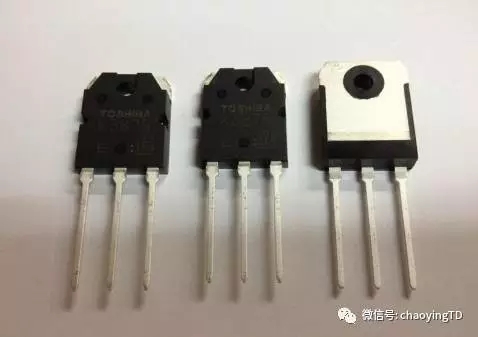
The first report on the fabrication of metal-p-type diamond semiconductor FETs was published in 1999. With the development of microelectronic assembly technology, micron-sized metal-p-type diamond semiconductor FET research has become a hot research topic. On the basis of the predecessors, Ulm's research team published a report on the results of a computer simulation of a metal-p-type diamond semiconductor FET with excellent performance and high stability. The report states that the theoretically operable temperature of the fabricated FET reaches 1000 ° C, the cutoff frequency can reach 30 GHz, and the simulated output power density reaches 30 W·cm -1 . In 2008, the group published the latest literature indicating that they actually prepared There is a certain gap between the sample and the simulation result, and the cutoff frequency is much smaller than the theoretical value.
Field emission (FE) materials, Pho-to-emission (PE) materials, Secondary electron emission (SEE) materials, Ion induced electron emission (IIEE) materials, etc. The principle of internal electron escape surface is successfully prepared, but the induction mechanism is different. The latter two mainly use photon energy and initial electron energy to make the internal electrons of the crystal obtain larger kinetic energy and escape above the surface barrier; the former The energy of the diamond surface barrier is reduced by a strong electric field, and the electrons inside the diamond crystal are released by the quantum tunneling effect.
The research objects in this area are generally hydrogen-terminated Bp-type diamonds, as well as some P-doped n-type diamond semiconductors and surface-hydrogenated diamond film samples. Through research, the electron emission intensity will have a certain attenuation with time, the main reason is the loss of surface hydrogen. This discovery has had a detrimental effect on the long-term application of diamond-based electron emitters.
The diamond surface is subjected to hydrogen plasma sputtering to form a hydrogen terminal surface. In 1989, Landstrass reported for the first time that the hydrogen terminal surface exhibited p-type conductivity, and others later confirmed this finding. In 1997, Hayashi et al. found that the surface electrical properties of B-containing diamond films after hydrogen surface treatment showed the same change law as undoped diamond. Hydrogen-terminated diamond materials have been used as field-emitting transistors for more than 10 years. The MIT research team first analyzed the emission surface of diamonds and found Fermi energy after B-doping and N-doping. The electron emission characteristics near the stage; then they prepared the diamond material used as the field emission cathode, investigated the contact current between the metal and diamond, and proposed the electron release mechanism of the diamond in vacuum.
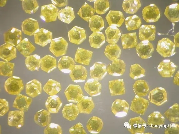
The measurement of electron current density is generally detected by time-of-flight mass spectrometry (TOF). It is also feasible to use TOF to analyze the electronic flight time of TOFs. However, it should be noted that due to the limitation of measurement conditions, it is difficult to compare the values ​​of TOFs, because the initial energy of ions is different when leaving the ion source, so that the ions with the same mass-to-charge ratio reach a certain time of the detector, resulting in resolution. Decrease in ability. Of course, comparing the values ​​of TOFs in a report published in the same group is still meaningful.
The diamond lattice prepared by ion sputtering method also exhibits good field emission characteristics. The nano-diamond pyramidal lattice is better on the diamond single crystal or single crystal Si wafer.
Diamond PE research may be the earliest. Himpsel et al. studied the defect morphology and energy level of the (111) plane of B-doped diamond single crystal by light emission method for the first time. Another important work in this field is that Bradis and Pate studied the hydrogen terminal by this method. The defect level and surface structure of the surface containing B diamond. Further research suggests that the hydrogen termination method has a huge impact on the stability of CVD diamond films.
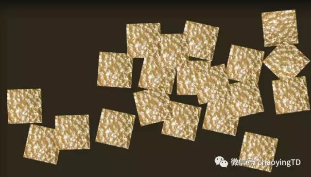
Diamond has a high SEE coefficient, which was confirmed in the 1990s. The range of diamond sizes currently studied has been reduced from micron to nanometer. In the early 1990s, some people conducted experimental studies on the SEE characteristics of diamond films, and found that the SEE coefficient of diamond films is relatively large (up to 10). Subsequently, the SEE characteristics of different doped diamond films were studied. In the case of erbium doping, the SEE coefficient of diamond films was as high as 55 at 5 kV. In the late 1990s, the SEE coefficient of surface hydrogenated diamond films was investigated. The study found that the hydrogenated diamond film has a higher SEE coefficient than the erbium-doped diamond film.
At the beginning of the 21st century, the US Naval Laboratory conducted an experimental study on the transmission SEE coefficient of diamond films, and found that the diamond electron film has a secondary electron transmission coefficient of 10 in the case of more than a dozen kilovolts. The biggest problem with SEE is still the instability of diamond hydrogenated films. Many of the reports in recent years have been the destructive study of hydrogenated surfaces by different factors.
IIEE has an important defect, which easily leads to the graphitization of diamond. Therefore, although it has been pointed out that diamond has good IIEE characteristics, it has great application potential in plasma display, but currently it is looking for suitable bombardment ions to avoid diamond. Graphitization is still an important research bottleneck.
3. Research and application in ultraviolet detectors
Diamond has very good electrical properties, such as a band gap of 5.5eV, a resistivity of 1010 Ψ·cm or more, and a dielectric constant of 5.5. Theoretically, diamond can be used as a detector in extremely harsh radiation environments. Material. Research on diamond radiation detectors began very early, from natural diamonds to HPHT diamonds to CVD diamond films.
The development of diamond ultraviolet detectors has always been an important research content of national defense and space science and technology. Many foreign scientific research institutions have started research work in this area. Zhou Haiyang has made a detailed summary and summary. At present, the diamond detector is not satisfactory because of the signal problems caused by impurities and defects of polycrystalline materials. The breakthrough of diamond detectors actually depends on the quality of synthetic diamond. The detector signal prepared by synthetic diamond is better than natural diamond. Small, the spatial uniformity of response needs to be improved.
4. Research and application of single photon source for quantum computer
The development of efficient single photon sources is an important basis for quantum information processing such as quantum computing, quantum cryptography and quantum networks. Single photon control is an important means of quantum computer construction and encryption. The fluorescence emission wavelength of diamond NV defects is 637 nm, and a single diamond containing Ni impurities has fluorescence emission in the near infrared, and both of these defects have the potential to become a highly efficient single photon source.
In particular, the single photon controllability of diamond NV defects has become a hot topic in recent years, and even research in this field is currently in its infancy. Many research groups have published many reports in this regard. J. Wrachtrup described in detail in his report the study of the energy levels and electron spin states of NV defects, and the research process of using NV defects as single photon sources. Made a summary summary and outlook. J. Wrachtrup also believes that not only these two defect luminescence may become an important source of single-photon emission, but also the possibility of other defects in diamond luminescence, and the development of nanotechnology provides more controllability of defects. .
5. Research and application of B diamond film electrode
In the application research of diamond functional materials, the research of B diamond film electrode (BDD) is almost the most extensive, and the number of published reports can also be ranked in the forefront of other research directions. BDD electrodes have many advantages in biological, electrochemical, environmental chemistry, especially waste treatment.
6. Research and application of acoustic packaging materials electronic packaging materials
The information industry has put forward higher and higher requirements for the performance of substrates and packaging materials such as high thermal conductivity, low thermal expansion coefficient, low dielectric constant and good thermal stability. Diamond has a high thermal conductivity, excellent insulation properties, and a low dielectric constant. These characteristics are in line with the basic requirements of electronic packaging materials. In fact, in acoustic materials, diamond films generally exist as substrate materials, and the applications are still excellent in properties such as high thermal conductivity.
The layer structure is the material of choice for high frequency surface acoustic wave devices. Diamond/ZnO composites have always been the hottest direction for the study of acoustic materials. This research has been studied for more than ten years from theoretical calculations to preparation methods.
The piezoelectric response time (110 min/V) of V-doped ZnO thin film/diamond composite reported by Tsinghua University is more than one order of magnitude higher than that of undoped materials, and has a better preferred orientation on diamond (002) crystal plane. . At present, the preparation and polishing of high-quality piezoelectric films and large-area diamond films are still the main obstacles restricting the development of diamond high-frequency SAW devices. It seems that with the improvement of film preparation technology and polishing technology, diamonds in high-frequency surface acoustic waves Device applications will become more widespread.
The diamond film is generally applied as a heat transfer medium on an alumina ceramic substrate. The Shanghai University of China has reported on dielectric loss and thermal conductivity. The report indicates that the thermal conductivity of the composite is five times that of alumina alone. In fact, the large-area preparation of thin films has always been a research problem, and the high cost of diamond films also restricts the development of research in this area.
The preparation method of diamond powder has been very mature, and the preparation of electronic packaging materials by using diamond powder has recently been reported. The chemical inertness of diamond under normal pressure has led researchers to study it as an important filler for composite materials. That is to say, many reports actually study the interface between diamond and other components in composite materials, such as wettability. Changes and so on. At present, the research on this aspect mainly involves diamond-Cu, diamond-Al, diamond-boron glass and other systems.
It is difficult to mention the thermal conductivity and dielectric loss performance of composite materials in these reports. It is possible that the actual dielectric constant of synthetic diamond is difficult to reach the theoretical value due to the presence of defects, but this does not hinder people's diamond electronic packaging materials. Research passion.
7. Outlook
Diamond integrates mechanical, electrical, thermal, optical and other excellent properties, making it widely used in high-tech fields, especially in electronic technology. Although the development and research of diamond functional materials is difficult to prepare in large areas, defect control is difficult. It is still the most promising new electronic material recognized by the high cost of preparation. At the same time, because it is an excellent high-temperature semiconductor material, it plays an important role in the development of semiconductor devices. In addition, with the gradual development of the thermal and electrical properties of diamonds, the development of VLSIs and ultra-high-speed integrated circuits will enter a new era.
Recoil Springs,Steel Spring For Slap Band,Plastic Torsion Springs,Flat Wire Recoil Spring
Professional Recoil Springs manufacturer is located in China, including Steel Spring For Slap Band,Plastic Torsion Springs,Flat Wire Recoil Spring, etc.
We are factory, we had made these products 15 years, we can give you good serve and quality. Hope to business with you!
Recoil Springs,Steel Spring For Slap Band,Plastic Torsion Springs,Flat Wire Recoil Spring
Shenzhen Lanejoy Technology Co.,LTD , https://www.brassinsert.net